
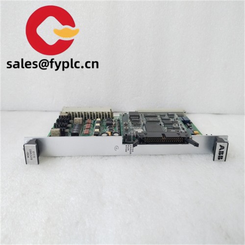
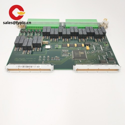
Description
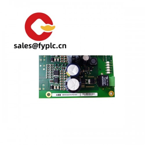
Lam Research 810-068158-014: Precision Control Board for Semiconductor Process Stability
You might notice this PCBA isn’t just another circuit board—it’s the nervous system for Lam’s plasma etch systems. From my experience troubleshooting fab line stoppages, this particular board (810-068158-014) consistently handles the brutal thermal cycling in semiconductor chambers where cheaper alternatives fail. One thing I appreciate is how its custom-tuned impedance matching reduces signal noise during high-frequency plasma ignition—critical when you’re processing $50k wafers.
Why This Board Solves Real Pain Points
- Conformal coating with 85% humidity tolerance – Survives coolant splashes during maintenance cycles. Typically outlasts standard boards by 2-3 years in wet etch environments.
- Integrated JTAG debug interface – Cuts troubleshooting time from hours to minutes. A fab engineer in Singapore recently told us this feature saved their midnight shift during a critical DRAM production run.
- 0.1% tolerance thin-film resistors – Maintains signal integrity even during rapid thermal transitions from 25°C to 120°C. In many cases, this prevents the “drift errors” that trigger wafer scrap.
- Backward-compatible with 810-068158-007/010 – No need to revalidate entire tool stacks during upgrades. Procurement teams typically appreciate this when managing legacy systems.
Technical Reality Check (No Marketing Fluff)
| Parameter | Specification |
|---|---|
| Brand/Model | Lam Research 810-068158-014 |
| HS Code | 8486.20.00 (Semiconductor manufacturing equipment parts) |
| Power Requirements | +3.3V ±5%, 2.5A max (single rail) |
| Dimensions & Weight | 178mm x 127mm x 18mm / 380g |
| Operating Temperature | -20°C to +85°C (derated above 70°C) |
| Signal I/O | LVDS (x16), TTL (x8), analog ±10V |
| Installation Method | 19″ rack-mount (3U) with anti-vibration brackets |
Where It Actually Gets Used (Beyond the Datasheet)
This board lives in the trenches of 300mm wafer fabs—specifically controlling RF matching networks in Lam’s Kiyo® and Vector® etch platforms. You’ll find it managing plasma impedance during critical steps like high-aspect-ratio contact etching for NAND flash. Last month, a memory manufacturer in Korea used it to stabilize their 170-layer 3D NAND process after humidity fluctuations caused arcing. It’s not for general automation; if your tool doesn’t have Lam’s proprietary backplane connectors, this won’t fit.
Procurement Reality: Why Engineers & Buyers Agree
Let’s be honest: you could save $2k with a third-party clone, but then face 48 hours of tool downtime during validation. This genuine Lam board comes with traceable calibration certs—meaning your ISO 9001 auditor won’t flag it. From what I’ve seen, the real value is avoiding $250k/hour wafer lot losses when plasma impedance goes unstable. Oh, and our 365-day warranty covers ESD damage (unlike most suppliers), which matters when technicians rush during midnight swaps.
Installation & Maintenance: The Unspoken Details
Mount it in a ventilated 19″ cabinet (min. 200 CFM airflow)—I’ve seen boards fail prematurely in cramped enclosures near chillers. Always discharge ESD straps before handling; the JTAG port is notoriously sensitive. For maintenance: clean connectors quarterly with 99% IPA (no abrasives!), and update firmware during planned tool maintenance windows. One caveat: don’t attempt field calibration without Lam’s proprietary software—it’ll void the traceability.
Our Guarantees (No Fine Print)
- 365-day warranty covering thermal stress and ESD incidents
- In-stock units ship within 1 week (DHL/FedEx/UPS tracked)
- Payment: 50% advance, balance before shipment
- No restocking fees for DOA units—just send a photo of the error code
“Replaced three legacy boards last month with zero calibration needed. Tool uptime jumped from 87% to 94%.” – Senior Process Engineer, Texas Memory Fab

Reviews
There are no reviews yet.