

Description
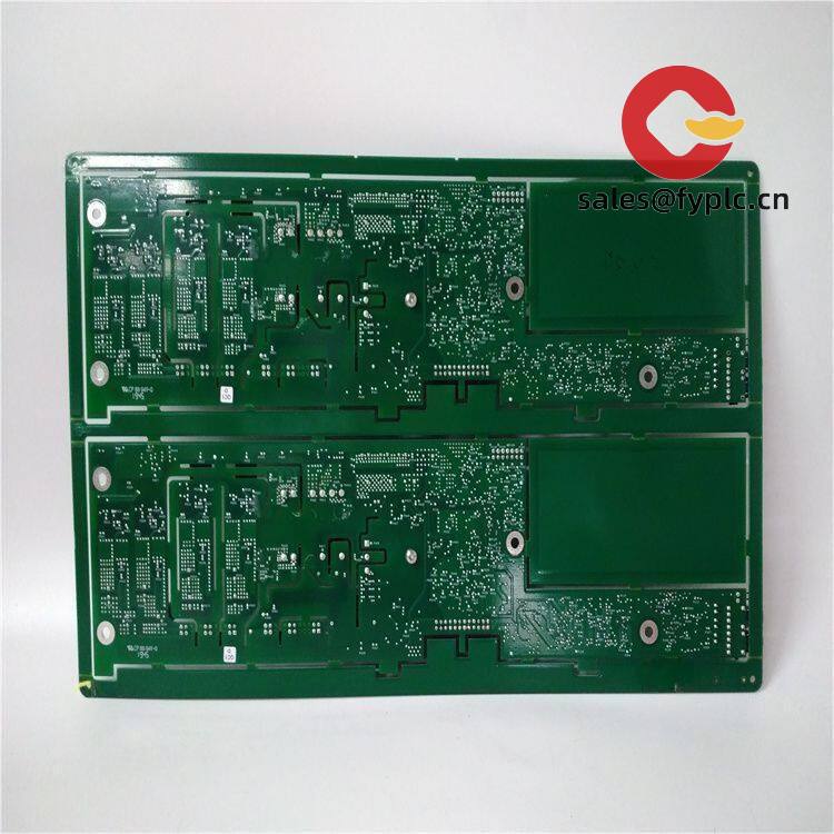
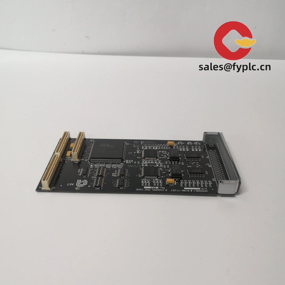
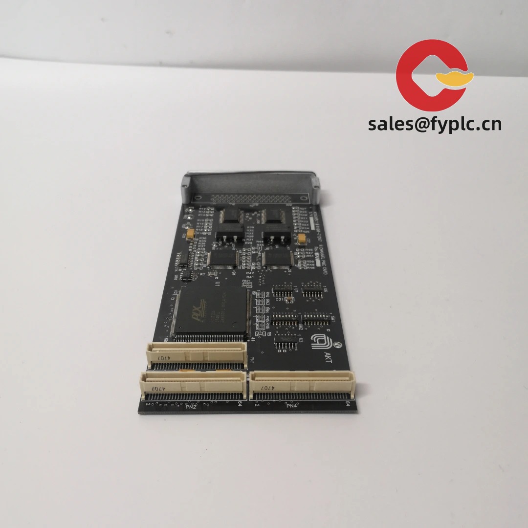
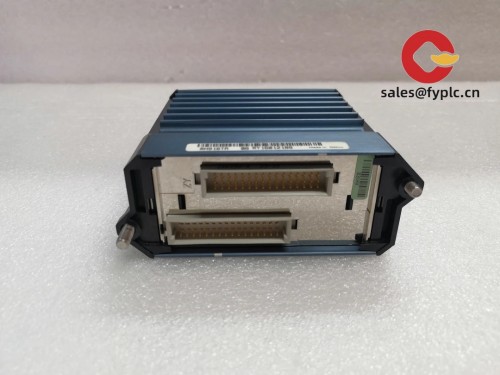
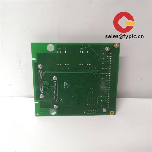
Applied Materials 0010‑23715 PMAX Emissometer Assembly
Technical Specifications
- Product Model: 0010‑23715
- Brand: Applied Materials (AMAT)
- Warranty: One Year
- Input Voltage: 24 V DC auxiliary power supply
- Operating Temperature: 15 °C ~ +65 °C (chamber‑adjacent clean‑room environment)
- Storage Temperature: ‑20 °C ~ +70 °C
- Response Time: <100 ms optical measurement update
- Protection Class: IP30 (clean‑room equipment assembly)
- Accuracy Class: Pyrometer grade, ±2 °C temperature measurement accuracy
- Output Frequency: Not applicable
- Rated Current: 1.2 A max @24 V DC
- Device Type: PMAX emissometer / pyrometer sensor assembly
- Measurement Principle: Infrared optical emissivity & wafer temperature measurement
- Optical Interface: Fiber‑optic light path for chamber non‑contact measurement
- Signal Interface: Analog + digital serial communication to tool host controller
- Compatibility: Applied Materials Centura / Endura PVD process chamber platforms
- Compliance: SEMI S2‑0703 semiconductor‑equipment safety standard
- Humidity: 5‑80 % RH, non‑condensing, clean‑room grade
- Weight: 1.1 kg
- Dimensions: 220 × 130 × 85 mm
Product Overview
The 0010‑23715 is a PMAX emissometer assembly from Applied Materials, a critical optical metrology spare‑part for physical‑vapor‑deposition (PVD) wafer‑processing chambers. It performs non‑contact infrared emissivity detection and real‑time wafer‑substrate temperature measurement during metal‑deposition process cycles.
Using fiber‑optic pickup, the assembly captures thermal radiation from the wafer surface inside vacuum process chamber, computes real‑time emissivity compensation and outputs accurate wafer‑temperature readings to the tool main controller. This measurement data is used for closed‑loop heater‑power regulation to stabilize wafer temperature, ensuring PVD‑film deposition repeatability and wafer‑to‑wafer process consistency. Precision optical components are sealed against particle contamination for clean‑room fab operating conditions. Original OEM production is discontinued; widely supplied as refurbished, rebuilt or new‑old‑stock spare parts for semiconductor‑fab equipment maintenance.
Application Notes
‑ Designed exclusively for AMAT Centura and Endura PVD processing chambers. ‑ Optical fiber path must be handled with extreme care; avoid bending below minimum bend radius to prevent internal fiber damage. ‑ Strict ESD control is required during handling and replacement. ‑ Install inside class‑1 / class‑10 clean‑room environment; prevent dust and particle contamination on optical window surfaces. ‑ Post‑replacement optical calibration is mandatory to restore rated measurement accuracy. ‑ Do not expose to corrosive process gases or condensation. ‑ Typical deployment: semiconductor wafer fabs for PVD metal‑deposition tool maintenance, chamber‑retrofit and spare‑part inventory.







Reviews
There are no reviews yet.