
Description
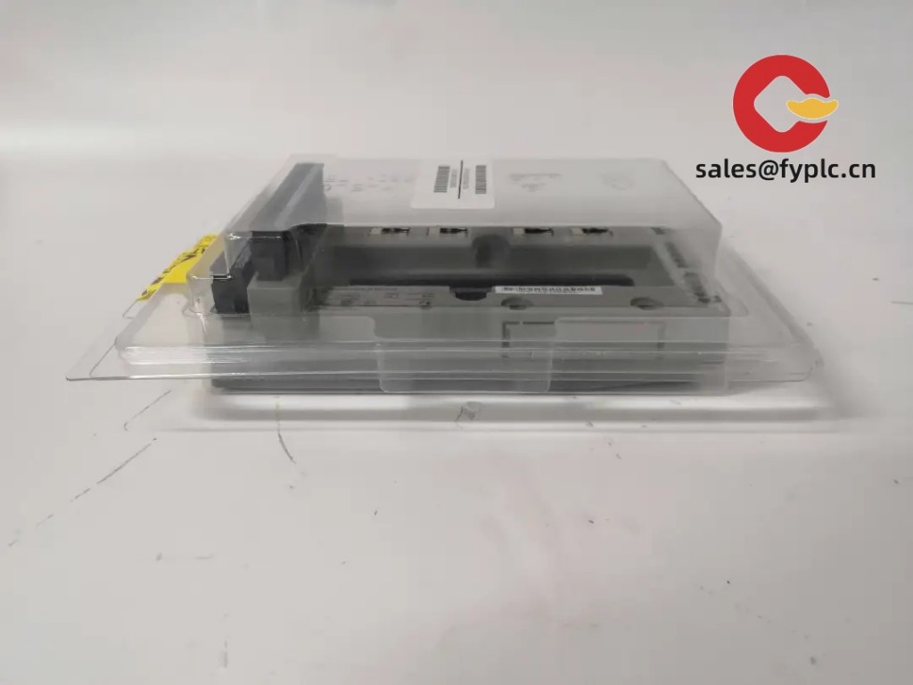
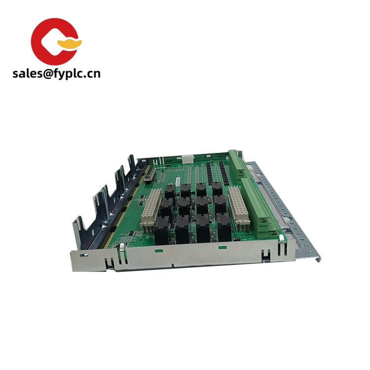
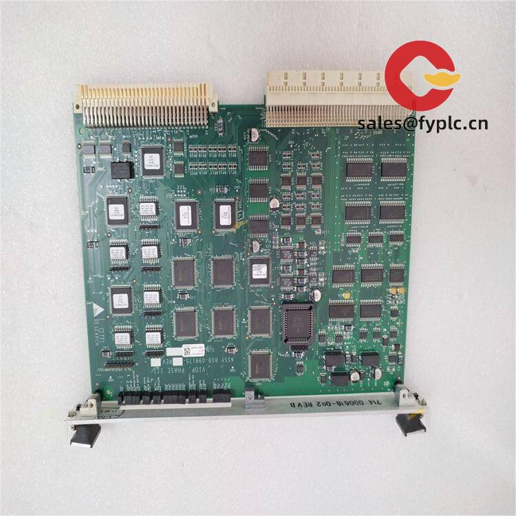
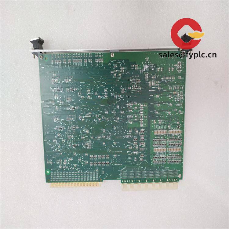
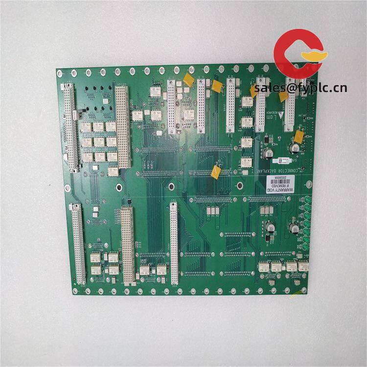
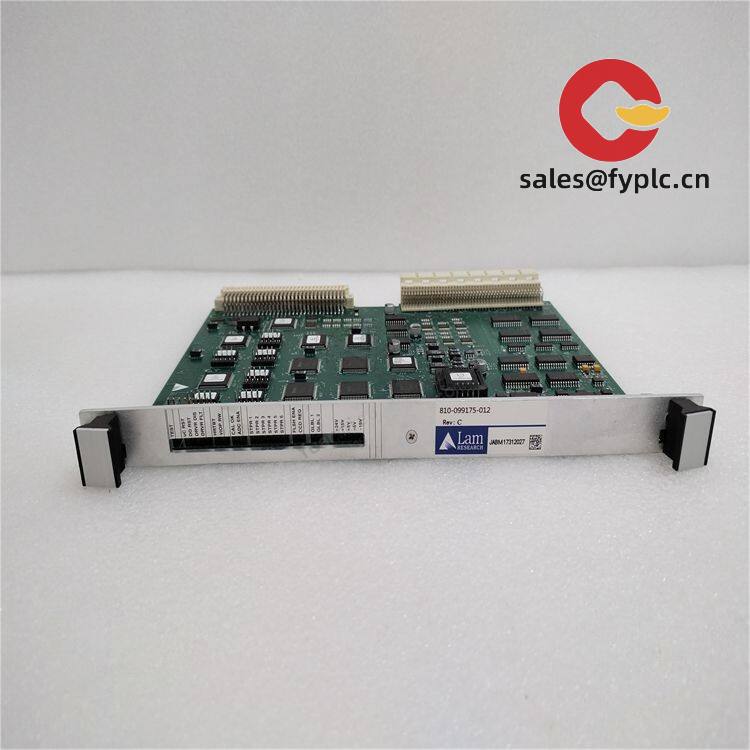
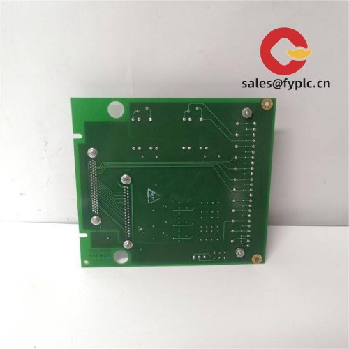
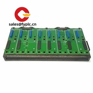
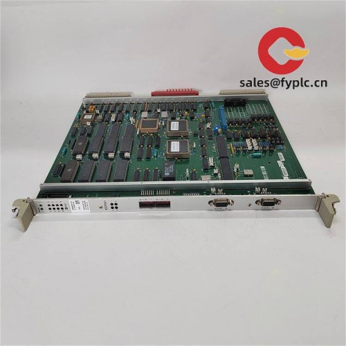
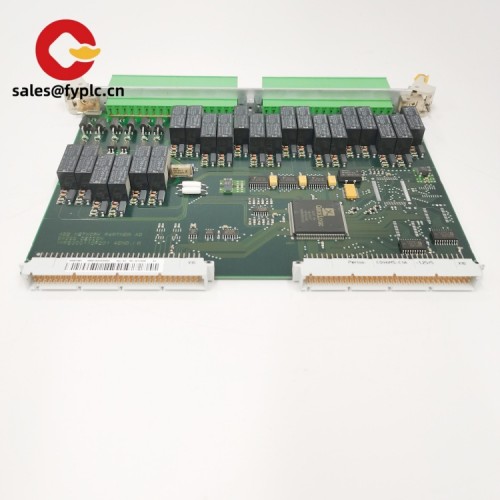
LAM 853‑245622‑014 Process Control PCB Board
Technical Specifications
- Product Model: 853‑245622‑014
- Brand: LAM Research
- Warranty: One Year
- Input Voltage: 5 VDC / ±12 VDC rack logic supply
- Operating Temperature: 10 °C ~ +50 °C
- Storage Temperature: ‑40 °C ~ +70 °C
- Response Time: Signal processing <1 ms
- Protection Class: IP20 equipment‑internal plug‑in PCB
- Accuracy Class: Semiconductor‑equipment signal‑processing grade
- Output Frequency: Not applicable
- Rated Current: 0.60 A typical board consumption
- Function: Process interface control PCB for LAM semiconductor etch‑tool equipment; performs analog‑signal conditioning, discrete‑I/O buffering and internal equipment‑bus communication for wafer‑processing chamber‑control
- System Compatibility: LAM etch processing tool platform
- Diagnostics: On‑board status test‑points for equipment‑troubleshooting
- Certifications: CE
- Humidity: 5‑80 % RH, non‑condensing
- Weight: 0.33 kg
- Dimensions: Standard LAM tool internal PCB form‑factor
Product Overview
853‑245622‑014 is proprietary interface circuit board for LAM semiconductor wafer‑etch processing equipment. It handles chamber sensor‑signal conditioning and equipment‑internal digital‑I/O buffering to support plasma‑etch process‑sequence execution. This original OEM semiconductor‑tool spare‑board is end‑of‑production; available as refurbished and surplus spare parts for fab‑equipment preventive‑maintenance and tool‑repair projects.
Application Notes
‑ Install inside designated LAM tool electronics‑chassis slot. ‑ Strictly observe ESD anti‑static handling requirements for semiconductor‑grade PCB assembly. ‑ Match board hardware revision to tool‑software revision. ‑ Typical deployment: semiconductor‑fab etch‑tool spare‑part stocking.

Reviews
There are no reviews yet.